AVR Timer programming Revision as of 17:05, 21 March 2016 by Raghavendra (Talk | contribs)
Contents
Basics
Timers come in handy when you want to set some time interval like your alarm. This can be very precise to a few microseconds. Timers/Counters are essential part of any modern MCU. Remember it is the same hardware unit inside the MCU that is used either as Timers or Counter. Timers/counters are an independent unit inside a micro-controller. They basically run independently of what task CPU is performing. Hence they come in very handy, and are primarily used for the following:
- Internal Timer: As an internal timer the unit, ticks on the oscillator frequency. The oscillator frequency can be directly feed to the timer or it can be pre-scaled. In this mode it used generate precise delays. Or as precise time counting machine.
- External Counter: In this mode the unit is used to count events on a specific external pin on a MCU.
- Pulse width Modulation(PWM) Generator: PWM is used in speed control of motors and various other applications.
Atmega32 has 3 timer units, timer 0, timer 1 and timer 2 respectively. Let us start our exploration with timer 0.
Timer 0 Basics
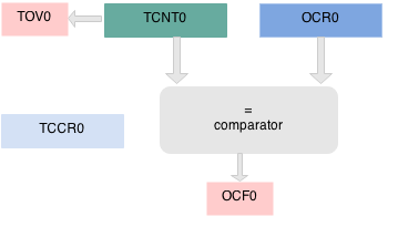
Timer 0 is a 8 bit timer. It basically means it can count from 0 to 2^8 255. The operation of timer 0 is straight forward. The TCNT0 register hold the timer Count and it is incremented on every timer "tick". If the timer is turned on it ticks from 0 to 255 and overflows. If it does so, a Timer OverFlow Flag(TOV) is set.
You can as well load a count value in TCNT0 and start the timer from a specific count. Another interesting feature is that a value can be set in the Output Compare Register (OCR0), and whenever TCNT0 reaches that value, the Output Compare Flag (OCF0) flag is Set.
| TCNT0 | D7 | D6 | D5 | D4 | D3 | D2 | D1 | D0 | |||||||
|---|---|---|---|---|---|---|---|---|---|---|---|---|---|---|---|
The configuration of the Timer can be set using the TCCR0 register shown below. With this you can basically select two things:
- The Frequency of the Clock Source with CS02, CS01, CS00 bits.
- The mode of the timer. For the first example we will use it in normal mode where it ticks from zero to the highest value(255)
| TCCR0 | D7 | D6 | D5 | D4 | D3 | D2 | D1 | D0 | |||||||
|---|---|---|---|---|---|---|---|---|---|---|---|---|---|---|---|
| FOC0 | WGM00 | COM01 | COM00 | WGM01 | CS02 | CS01 | CS00 | ||||||||
| D2 | D1 | D0 | Clock Source |
|---|---|---|---|
| CS02 | CS01 | CS00 | Freq |
| 0 | 0 | 0 | No Clock (Stopped) |
| 0 | 0 | 1 | Clk |
| 0 | 1 | 0 | Clk/8 |
| 0 | 1 | 1 | Clk/64 |
| 1 | 0 | 0 | Clk/256 |
| 1 | 0 | 1 | Clk/1024 |
| 1 | 1 | 0 | Clk/T0-Falling edge |
| 1 | 1 | 1 | Clk/T0-Rising Edge |
| D6 | D3 | PWM |
|---|---|---|
| WGM00 | WGM01 | Mode |
| 0 | 0 | Normal |
| 0 | 1 | CTC (Clear timer on compare match) |
| 1 | 0 | PWM (Phase correct) |
| 1 | 1 | Fast PWM |
The Timer/counter Interrupt Flag Register(TIFR) holds the two basic flags we need the TOV and OVF. Other bits correspond to the timer interrupts, which we will look at in another tutorial.
| TIFR | D7 | D6 | D5 | D4 | D3 | D2 | D1 | D0 | |||||||
|---|---|---|---|---|---|---|---|---|---|---|---|---|---|---|---|
| OCF2 | TOV2 | ICF1 | OCF1A | OCF1B | TOV1 | OCF0 | TOV0 | ||||||||
Timer 0 Example
Let us do a simple example to set the timer 0 in normal mode and toggle an LED when it overflows. To accomplish this, we'll do the following steps.
- Load TCNT0 with 0x00
- Set CS00 and CS02 bits in TCCR0 register. This will start the timer at Clk/1024 speed. We will calculate the tick time in just a moment.
- Monitor the TOV0 flag in the TIFR0 register to check if the timer has over-flowed and toggle the LED status.
How much delay does it generate?
Okay, lets calculate. The Explore Ultra AVR dev board comes with a 16MHz on board crystal and the fuse bits are set appropriately. $$Ftimer = 16MHz/1024 = 15.625KHz $$ $$Ttick = 1/ 15.625K = 64 micro seconds$$ $$Ttotal = 64us x 255 = 16mSec$$
Timer 1
| TCNT1H | TCNT1L | ||||||||||||||
|---|---|---|---|---|---|---|---|---|---|---|---|---|---|---|---|
| D15 | D14 | D13 | D12 | D11 | D10 | D9 | D8 | D7 | D6 | D5 | D4 | D3 | D2 | D1 | D0 |
| TCCR1A | D7 | D6 | D5 | D4 | D3 | D2 | D1 | D0 | |||||||
|---|---|---|---|---|---|---|---|---|---|---|---|---|---|---|---|
| COM1A1 | COM1A0 | COM1B1 | COM1B0 | FOC1A | FOC1B | WGM11 | WGM10 | ||||||||
| TCCR1B | D7 | D6 | D5 | D4 | D3 | D2 | D1 | D0 | |||||||
|---|---|---|---|---|---|---|---|---|---|---|---|---|---|---|---|
| ICNC1 | ICES1 | - | WGM13 | WGM12 | CS12 | CS11 | CS10 | ||||||||
| TIFR | D7 | D6 | D5 | D4 | D3 | D2 | D1 | D0 | |||||||
|---|---|---|---|---|---|---|---|---|---|---|---|---|---|---|---|
| OCF2 | TOV2 | ICF1 | OCF1A | OCF1B | TOV1 | OCF0 | TOV0 | ||||||||


